Add to Cart
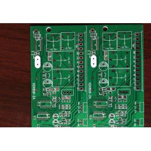
Car Product PCB for Vehicle Navigation PCBA Board / Printed Circuit Board
Product Description
| PCB Description | Our PCB Board Capability |
| PCB Surface Finishes | electrolytic nickel-gold, HASL(Lead Free, ENIG (Electroless Nickel/Immersion Gold, Carbon Ink, Golden Fingers, OSP (Entek, Immersion Tin, Immersion Silver |
| PCB Max. Size | 1200mm×600mm |
| PCB Min. Size | 5mm×5 mm |
| Bow & Twist Tolerance | Single Side≤1.0%,Double Side≤0.7%, Muti-Layer≤0.5% |
| Min. Board Thickness & Tolerance | 0.2mm±0.08mm |
| PCB Min. trace/spacing | Tin board:0.2mm±20%(8mil±0%) |
| gold board:0.075mm±20%(3mil±0%) | |
| Copper to Board Edge Spacing | 0.5mm(20mil) |
| Hole to Trace Spacing | 0.3mm(12mil) |
| Min. Hole Diameter | 0.2mm±.076mm(8mil±3mil) |
| Min. Hole Clearance | 0.4mm±.076mm(16mil±3mil) |
| Copper Thickness on Hole Wall | 20-25um(0.79mil-1.0mil) |
| Hole Location Tolerance | ±0.076mm(l±3mil) |
| Min Diameter of Punching Hole | FR-4 board thickness≤1.0mm(40mil):1.0mm(40mil) |
| FR-4 board thickness 1.2-3.0mm(48-120mil):1.5mm(60mil) | |
| PCB Min. Punching Slot | FR-4 CEM-3 board thickness≤1. 0mm(40mil):0.8 mm×0.8 mm(32mil×32mil) |
| FR-4 board thickness1.2-3.0mm(48-120mil): 1.0 mm×1.0 mm(40mil×40mil) | |
| Trace width variation | ±0.076mm(±3mil) |
| Outline Tolerance | Routing:±0.1mm (±4mil) ,Punching:±0.05mm (±2mil) |
| V-CUT Registration Tolerance±0.2mm (±8mil) | |
| PCB BOARD Type | Single-sided, double-sided, multi-layer |
| Major Material | FR-4, CEM-1,CEM-3, high frequency laminates, Aluminum, NiFe-based, copper base |
| PCB BOARD Thickness | 0.2-3.5mm |
| Base Copper Thickness | 11um 35um 70um 105um |
| Max. aspect ratio(board thickness: hole size) | 8:1 |
| V-Cut Angle Tolerance | ±5° |
| V-Cut Board Thickness | 0.4mm -3.2mm(16mil -128mil) |
| Min SMT Pitch | 0.3mm(12mil) |
| Min. Component mark | 0.15mm(6mil) |
| Min. width of annular ring(finished) | 0.15mm(6mil)/side |
| Min pad opening | 0.076mm(3mil) |
| Min S/M Bridge | ±0.076mm(±3mil) |
| carbon ink board manufacturing capability:1.Impedance Control:20K±10% 2.Hardness:6H 3.bearable friction times :above 200000 times | |
What we need:
Please tell us the information as below:
| NO. | Items | NO. | Items |
| 1 | Board for what product | 8 | Surface Finish |
| 2 | Number of Layers | 9 | Board Material |
| 3 | Copper Thickness(um) | 10 | Board Thickness(um) |
| 4 | Solder Mask Color | 11 | PCB Dimensions(mm) |
| 5 | Silk Screen Color | 12 | Min Finished Hole Size(mm) |
| 6 | Milling | 13 | Min Clearance(mm) |
| 7 | Min Track Width(mm) | 14 | Other special requirements |
| Packaging | Vacuum Packing with desiccant, Professional Export Carton. |
||
Delivery time |
Prototype | Mass production (above 30m) |
|
| 2L | Quick turn:24h Usual time:3-4days |
5-10days | |
| 4L | Quick turn:48 hours; Usual time:5-6days |
10-15days | |
| 6L | Quick turn:72 hours; Usual time:6-8days |
10-20days | |
| 8L | Quick turn:72 hours; Usual time:8-10days |
15-22days | |
| 10L | Quick turn:96 hours; Usual time:12-14days |
18-25days | |
| `` | `` | `` | |